MB85RC256V 32KB FRAM Memory
Contents
What is FRAM Memory?
Ferroelectric RAM also known as FRAM is a type of random access memory. It is non-volatile i.e. the memory contents are retained even when powered down. It is also not affected by magnetic interference.
A FRAM chip contains a thin layer of ferroelectric material. Ferroelectric materials have a natural electric polarization that can be reversed by applying an external electric field. This property is used in FRAM chips to produce large numbers of binary switches.
Flash memory (of USB memory stick fame) has a much higher memory cell density than FRAM so its per bit cost is lower. However FRAM memory is much quicker especially for writing and has a much better endurance (number of write cycles).
The MB85RC256V Chip


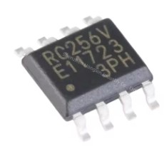
Fig 1 - The MB85RC256V 32KB FRAM chip
The MB85RC256V chip is the product of Fujitsu Semiconductor Ltd, a significant world player in FRAM design and manufacture.
FeaturesThe MB85RC256V has 32,768 bytes (32KB) of FRAM memory. As noted above FRAM memory is very durable. This chip is no exception with a reported read/write endurance of 1012 times/byte. Data retention is expected to be 95 years if the chip is kept at a temperature not exceeding 55 °c.
It has an operating power supply voltage of 2.7V to 5.5V so is immediately usable by both 3.3V and 5V powered microcontrollers. Power consumption is very low at a maximum current of 200 µA but realistically this reduces to around 120 - 150 µA when used by the typical microcontroller.
It is supplied in a choice of two different sized 8-pin SOP (Small Outline Package) packages. Dimensions of the two packages are:
- FPT-8P-M08 : 5.30mm x 5.24mm
- FPT-8P-M02 : 5.05mm x 3.9mm
The 8-pin pinout is simple:
- VDD, VSS : +ve power and ground respectively.
- A0, A1, A2 : I2C address configuration.
- SCL, SDA : I2C clock and data pins respectively.
- WP : Memory write protect
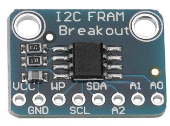
The SOP packaging isn't very breadboard friendly. Most hobbyists will use this chip on a breakout board where usually all eight pins are broken out.

Note: On the breakout board the chip's VDD pin has been renamed to VCC. The chip's VSS pin is now named GND.
The MB85RC256V chip has an I2C interface for all communications with the master device.
The I2C address is set using the A0, A1 and A2 pins. Each pin can be connected to either VCC (VDD) or GND (VSS) to give a possible eight different addresses. The following table matches the pin connections with the resultant address.
| A2 | A1 | A0 | Address |
|---|---|---|---|
| GND | GND | GND | 0x50 |
| GND | GND | VCC | 0x51 |
| GND | VCC | GND | 0x52 |
| GND | VCC | VCC | 0x53 |
| VCC | GND | GND | 0x54 |
| VCC | GND | VCC | 0x55 |
| VCC | VCC | GND | 0x56 |
| VCC | VCC | VCC | 0x57 |
The breakout boards come with all three pins connected to GND, so have a default I2C address of 0x50. Of course, since the A0, A1 and A2 pins are accessible on the board the address is easy to change if more than one of these is to be interfaced with the microcontroller.
Reading & Writing the MB85RC256V Memory
Accessing the memory of the MB85RC256V is simple. It is a linear flat byte addressable space with memory addresses that start at 0x00 and continue incrementally upwards to the last memory byte's address at 0x7FFF All reading and writing of memory is through the I2C interface.
The MB85RC256V maintains an internal Address Counter. This register contains the address of the next memory byte to be read or written. After each read or write operation the Address Counter is incremented automatically by the chip.
Memory addressing is circular. This means that the Address Counter rolls back to the first byte's address i.e. 0x00 if the last byte in memory has just been read or written.
The microcontroller master can write to the Address Counter but unfortunately can't read it. This doesn't particularly impact reading from memory. But it does add an extra administrative load on the user program during memory writes. This is discussed below.
Reading
Reading the FRAM memory is simple:
- Optionally write the memory address for the first read to the Address Counter. The 16-bit address is sent as two bytes; the MSB first followed by the LSB. If an address isn't sent to the Address Counter then the current value of this register is used.
- Read as many bytes as needed. The Address Counter auto-increments.
- Additional read requests can be made. Reading will continue at the next byte from the last read (or write) operation unless a new address is written to the Address Counter.
Writing
Writing to the FRAM memory is a little more complicated than the reading operation. The basic operation is:
- Prepare the write buffer:
- The first two bytes will always be the 16-bit address that will be loaded into the Address Counter.
- Any bytes to be written to memory following these first two bytes are then added. This optional. If none are provided than just the Address Counter is updated. This is the case when a read operation is to follow.
- Write the buffer which includes the 16-bit address as the first two bytes, followed by the optional data load.
- Any following write operations will need to start at Step 1. This means that for sequential writes the user program needs to always calculate the memory address for the start of the next write. Any new write operation must always provide the first memory address as the first two bytes of the buffer.
Other Stuff
Software Reset
It is possible to software reset the MB85RC256V. It involves an unusual sequences of HIGH/LOW pulses with both the SCL and SDA lines before sending the usual address & read/write sequence.
Most I2C libraries won't provide support for this. Those interested should consult the product datasheet where it's explained with an excellent timing diagram.
Write Protecting the Memory
It's possible to write protect the memory with a hardware feature on the chip.
The WP pin on the chip is normally held LOW with a pulldown resistor connected to GND. If this pin is pulled HIGH then any attempt to write to the memory will cause a program error. In the case of MicroPython an OSError exception is thrown.
The state of the WP pin does not affect the ability to read the memory. So, even though memory might be write protected it can still be read.
The memory write protect is volatile i.e. after the chip loses power it does not store the write protect status for when it is next powered up.
Device ID
Many chips with a digital interface have identification numbers burnt into the firmware during manufacture. The MB85RC256V is no exception. It has a readonly Manufacturer ID and Device ID.
The Reserved I2C address 0xF8 is sent followed by the MB85RC256V's own I2C address (e.g. 0x50). The master is then able to read three bytes.
The 12-bit Manufacturer's ID and the 4-bit Device ID is extracted; refer to the datasheet for details. A genuine Fujitsu chip will return these IDs:
- Manufacturer's ID : 0x00A
- Device ID : 0x5
MicroPython Driver for micro:bit
A MicroPython driver for the micro:bit can be found here.
This driver maintains a calculated memory address pointer that shadows the MB85RC256V's internal Address Counter. This very much simplifies writing to the FRAM memory. Repeated write operations can be performed without needing the client program to calculate and update the Address Counter each time.
The driver provides methods for the following:
- Read (calculated) and write the Address Counter
- Get the status of the last read or write operation.
- Clear the entire memory contents.
- Read and write blobs (binary data), strings, integers and floats.
- Set and reset memory write protection
- Return the Manufacturer ID and Device ID.