Logic Level Shifters
Contents
Introduction
There is a trend for microcontrollers and other digital electronics to be designed for powering with increasingly lower voltages. This reduces power consumption and hence also reduces waste heat buildup.
With that said there are still many devices out there that operate at 5V. This can be a problem if interfacing to the micro:bit's pins which are at 3.3V. Permanent damage can occur if a micro:bit pin is exposed to a voltage greater than about 3.6V.
Fortunately there are several solutions available to sort voltage disparity between different connected devices. This page briefly discusses four such options. The discussion is limited to logic level voltage shifting i.e. digital signalling.
NOTE : It is vitally important to understand that this discussion is limited to digital communications and is not relevant to analog pins.
Voltage DividerThe simplest solution is to use a voltage divider. This is simply two resistors connected in series with the output point between the two resistors - see Fig 1. This becomes a painful exercise if there are more than one or two pins involved.
There's heaps of online references that advise how to design a voltage divider for a specific application.
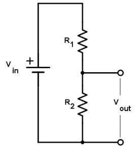
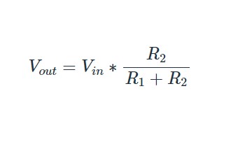
Fig 1 - Simple voltage divider circuit (https://www.allaboutcircuits.com/tools/voltage-divider-calculator/)
SN74LVC245
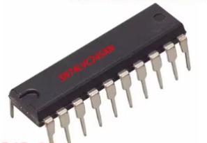
The SN74LVC245 chip is used to transmit and receive data between two different buses that may have different voltage levels. It has eight data pins on one side of the chip with matching pins on the other side.
The chip operates from a supply voltage of 1.65V to 3.6V. It can handle input voltages up to 5.5V. This makes it suitable for connecting the micro:bit's 3.3V with (e.g.) sensors that are supplied with 5V.
The downside to the SN74LVC245 is that it can only communicate in one direction at any given time. The chip has a DIR pin with the value (High or Low) of this pin determining the direction of communication. Thus to change the direction of communication between the two buses the value of the DIR pin must be inverted.
The SN74LVC245 is available in a DIP-20 package so is breadboard 'friendly'.
TXB0108EThe TXB0108E is a voltage-level translator produced by Texas Instruments. It is an 8-bit, bidirectional, non-inverting translator that uses two separate configurable power-supply rails.
It has a supply voltage range of 1.2V to 3.6V for VCCA and 1.65V to 5.5V for VCCB. So, again, this chip is suitable for interfacing the micro:bit's digital pins with a 5V peripheral.
The TXB0108E doesn't have a DIR pin as it is able to sense the direction of communication between buses. The direction of communication can change any time without any action to 'alert' the chip.
While the TXB0108E is not available in a DIP package, both it and the related TXS0108E can be acquired on breakout boards.
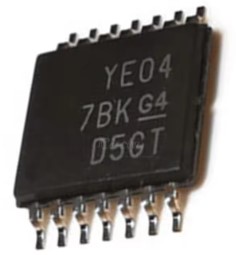
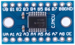
Fig 3 - TXB0108E chip and its related TXS0108E on a breakout board
BSS138 MOSFET Breakout Board
The BSS138 MOSFET allows two buses with wide voltage differences to reliable and rapidly communicate in either directions.
Breakout boards that have 4-channels and use BSS138 MOSFETs are readily available at almost throw away prices. These boards are extremely simple to use and require no driver software to operate.
These boards are by far the preferred solution for digital communications between devices operating at different voltages. They are commonly referred to as logic level shifters[1].
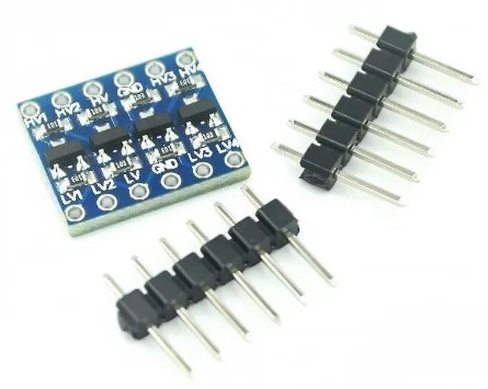
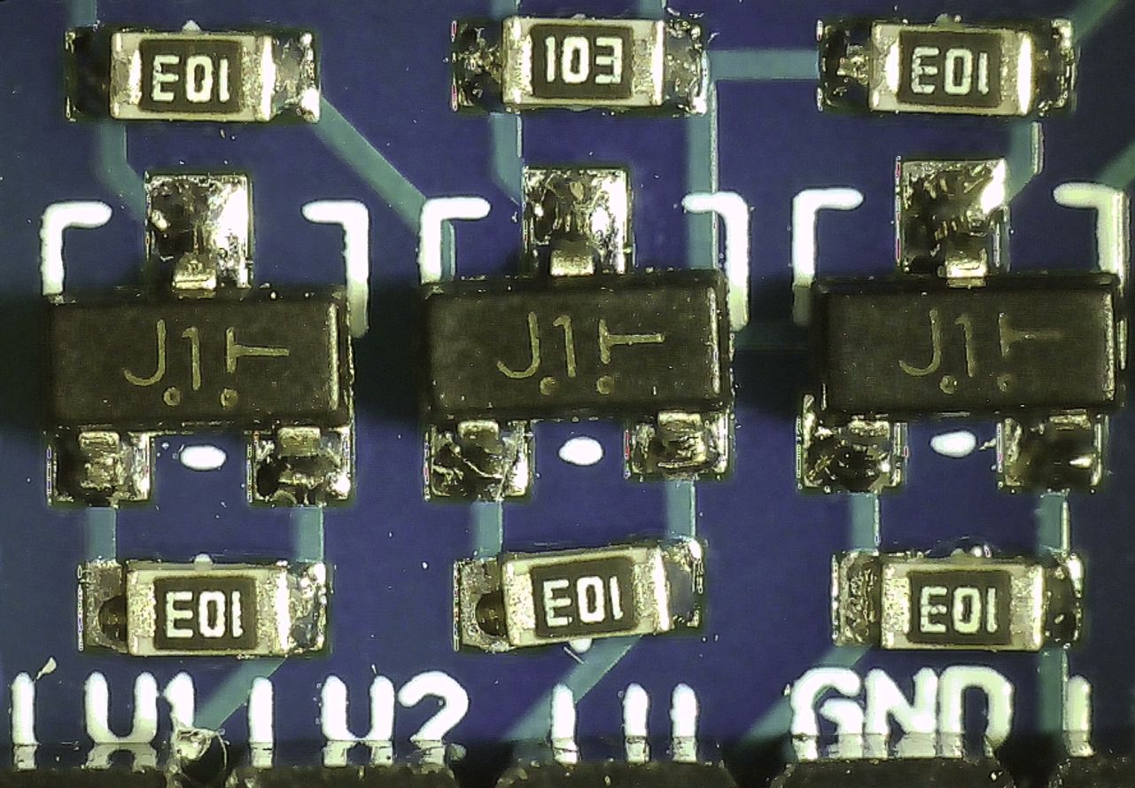
Fig 4 - Logic level shifter board with 4-channels. The voltage level conversion is done by BSS138 MOSFETs
Just about any serial protocol including SPI, I2C and proprietary protocols requiring the microcontroller to run 'bit bashing' algorithms will work with these boards.
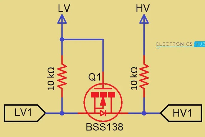
Just for completion, Fig 5 shows the circuit for one channel. Each logic level shifter board has four of these.
Logic Level Shifter Board Pinout
The pinout of the board is simple and intuitive:
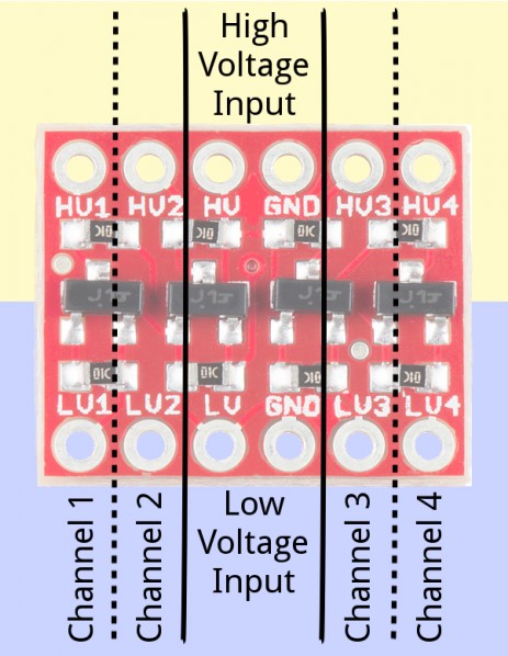
- HV : Connect the higher voltage (e.g. 5V)
- LV : Connect the lower voltage (e.g. 3.3V)
- GND : There are two GND pins; one for the higher voltage, one for the lower voltage. These pins are simple 'pass-throughs' which ensure the ground reference is common across both buses.
- LV1, LV2, LV3, LV4 : Lower voltage data pins. These are logic level switched to HV1, HV2, HV3, HV4 respectively
- HV1, HV2, HV3, HV4 : Higher voltage data pins. These are logic level switched to LV1, LH2, LH3, LV4 respectively
Example - DS1307 Real-time Clock
The DS1307 real-time clock chip is easy to use from a software perspective. However the designers of this chip built it for use with 5V power for reasons unknown. So, it can't be directly connected to a micro:bit.
This makes the DS1307 a good candidate for pairing with a logic level shifter.
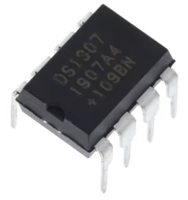
The following links show how the 5V-powered DS1307 can be interfaced with the 3.3V micro:bit:
- 5V power-supply options.
- DS1307 description.
- DS1307 MicroPython driver for the micro:bit. This includes full hookup instructions with example programs using the driver.